About 98% of all Integrated Circuits (ICs; chips) are made in Complementary Metal Oxide Semiconductor (CMOS) technologies. For a complete understanding of all disciplines of microelectronics that are involved in the creation of an IC, we offer this course. The course gives an overview of the basics, physics, fabrication, design and applications of CMOS ICs into the nanometer range. It also discusses technology/design scaling bottlenecks to and even beyond 22nm CMOS and is also meant to close the gap between the product development/engineering, design, test and technology communities.
A separate one-day course (Bits on Chips) is available for those with little or no technical background in integrated circuits, but who need an understanding of their complexity, their operation, their possibilities and limitations to better communicate with their technical contacts.
€ 1.600,00 excl. VAT
4 consecutive days
How participants recommend this training to others:
8.8
(average score of last 3 editions)
On request
Eindhoven or Nijmegen
A 4-day tutorial on the development of CMOS ICs. For IC designers, CMOS process engineers, lithography engineers and engineers working in electronic product development, who have to write and read IC specifications, test samples, discuss technical details with suppliers and customers, etc. and for others who need a thorough understanding of ICs.
The course addresses engineers with a broad range of functions who have in common that they need a thorough understanding of ICs, all disciplines of microelectronics covered are discussed in balance: Design -, product -, process - and lithography engineers, test and failure analysis engineers, package engineers, product engineers who supervise outsourced IC-development and have to read and write product specifications, engineers who discuss technical details with suppliers and customers.
Basic principles
MOS physics. Characteristics. Equations. Capacitances (short summary).
Geometry effects
Temperature behaviour. Subthreshold behaviour and leakage current mechanisms.
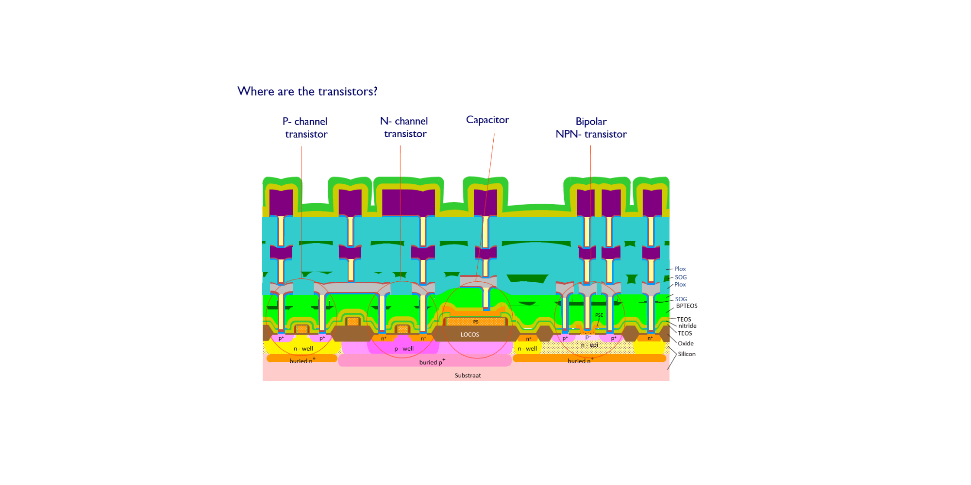
CMOS technology (including FinFet)
Lithography summary. Basic CMOS processing steps. From a basic nMOS process to a 22nm CMOS process.
CMOS design
Basic principles of electrical and logic design.
CMOS memories
Memory architectures, SRAM, DRAM, ROM, PROM, E(E)PROM (3-D), NAND- and NOR-flash memories, stand-alone and embedded memories.
VLSI and ASICs
Design flow. Hierarchy levels. IP cores. Re-use. ASICs.
Low-power / low leakage
Battery overview. Summary of existing technology and design options for low power and low leakage.
Robustness of ICs
Reliability and signal integrity issues. Latch-up, Punch-through, ESD protection circuits. Hot-carrier degradation. Electromigration. NBTI. Supply and substrate noise, power integrity, decoupling, cross-talk, noise margins, EMC, soft-errors and variability, etc.
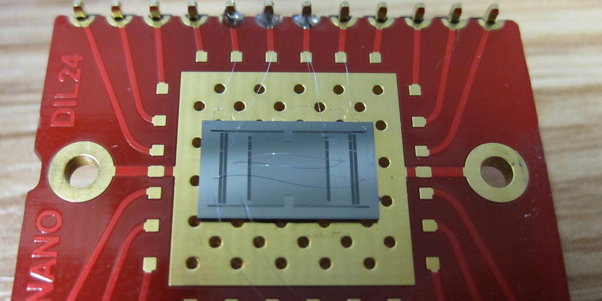
Testing, debugging, failure analysis and yield, packaging
Testing. Basics of yield and simple model. Packaging characteristics and trends, Diagnosis techniques, state-of-the-art failure analysis techniques. Repair, focused ion beam, etc.
Scaling trends and roadblocks
Scaling towards 22nm technologies and beyond. Speed and power trends. Design, masks and processing costs. Roadblocks and solutions. End of Moore’s Law!
Methods: lectures, exercises made during the course and during the evenings. Course material: book 'Nanometer CMOS ICs; 2017 edition'.
Participants receive a HTI certificate.
'The training is very good, you get the whole 'package' of IC design, production and applications.'
'Lecturer is great at explaining complex material with easy to follow examples, and also very knowledgeable. Excellent course!'
A comprehensive course to learn the basics of semiconductor physics, devices, processing, and of electrical process characterization.
Read more →
Introductory course on micro-electro mechanical systems (MEMS) with the basic theory, how MEMS are processed and various applications.
Read more →