Lectures supported by practical demonstrations and a final design case. Course notes.

Electronic devices become faster and smaller causing a strong increase of interference. The "fast edges" of modern electronic devices cause a lot of signal integrity (SI) problems. It is more and more difficult to use components within their specifications. The SI problems result in unexpected behavior of the hardware, reset problems, latch-ups, software hang-ups caused by the hardware and, last but not least, very noisy boards not compliant to FCC (USA), CISPR (EU) or VCCI (Japan).
This course stands out due to:
•highly applied, practical approach: Uses real hands-on modelling and simulation (HyperLynx);
•comprehensive coverage: Includes DDRx analysis, SerDes, timing, PI/EMC interactions;
•balanced SI with EMC/PI context: Teaches how SI fixes influence EMC and PI—interpreting cross-domain effects;
•very valuable for electronic designers, board layout experts, IC designers – bridging hardware/software perspectives;
•two experienced trainers who bring up-to-date knowledge and valuable insights to the course.
In this very practical course, the theory behind signal integrity is explained and illustrated, practical problems are modelled, simulated and analyzed, solutions are discussed, a way of working is proposed to minimize SI-problems. Electronic designers and board layout designers need to be aware of each other problems and approaches to solve and prevent SI-problems.
Demonstrations of analysis of problems are given with Hyperlynx. During the hands-on sessions, the course participants use Hyperlynx software to analyze system parts with SI problems and the effect of measures to reduce the SI-problems. Hyperlynx is a high-quality tool (in combination with technology files) for EMC, SI and PI-simulation. Note: the course is not a tool-training course.
Measures to improve SI cannot be done in isolation without paying attention to EMC and Power Integrity (PI). These SI measures can have a negative impact on EMC and PI. SI is the main topic of this course but potential negative consequences for EMC and PI are also discussed.
Note: The design of a power distribution network on a board is the main topic of the PI-course.
This training is available for open enrollment as well as for in-company sessions. For in-company sessions, the training can be adapted to your situation and special needs.
Objective
Creating awareness and delivering the knowledge that everything is interacting. Support participants in delivering the best quality products with components working within their specifications and environment.
After the course, the participant will:
•be able to recognize signal integrity problems of modern fast electronic systems;
•be able to analyze the signal integrity of a PCB;
•know and be able to apply methods to improve the signal integrity of a PCB;
•know IC characteristics that may cause signal integrity problems of a PCB;
•know a way of working to improve the SI;
•know which SI measures have a negative impact on EMC and PI;
•be able to tackle EMC problems in the beginning without degradation of the timing specs;
•know design partitioning in different noise classes for digital/analog mixed systems. Improve the SNR;
•be able to design for the EMC 3-dimensional electromagnetic environment;
•know how timing analysis is performed for DDRx;
•learn the analysis of the SerDes trending topology, Return and Insertion loss budgeting will be discussed.
Target Audience
This training is intended for systems architects, product designers, electronic designers as well as board layout designers and IC-designers. Required level BSc electronics electrical engineering and a working relation with EMC.
Program
Signal integrity problems may arise at many levels: within an IC, at the package level, on a PCB, at the backplane of boards, at inter-system communication.
There are issues that hold at various levels. This course concentrates on signal integrity on the PCB and around the interface between IC and PCB and is therefore highly relevant both for both board designers and IC designers. The examples applied during the course, however, stem from the PCB area. The course does not cover aspects like architectures for fast systems.
There are problems on signal integrity (and power integrity) that manifest themselves on a PCB but that should have been resolved on an IC. In case an IC strongly radiates (EMC), there are additional costs at PCB-level such as housing or metal shielding. It is possible that the required performance may still not be reached. To prevent these problems the board designer might choose a chipset from another supplier.
Furthermore, a relationship exists between the pinning of an IC and the number of layers of a PCB. For financial reasons there is a strong preference using a 4 layers board compared instead of 6 layers (costs are rising sharply with the number of layers). However, this gives demands on the pinning. If these demands are not handled properly, a 6-layer PCB might still be necessary because of SI reasons. An alternative is to select an IC from another supplier. The whole layer spectrum, up to 32 layers, is discussed.
Lessons:
•Signal integrity: high speed signal propagation, reflection, ringing, transmission-lines, termination, balanced lines, edge control, crosstalk, stack-up, simulation of high-speed nets;
•Power integrity: high speed power distribution, power planes topology, board stack-up planning, PCB production and materials, bypassing capacitors, embedded passives, power supply noise classes;
•IBIS modelling: creating IBIS models, modifying models, understanding the most important parameters of an IBIS model;
•EMC introduction: EMC compliance tests, emission, immunity to RF fields, EFT, bursts, pre-compliance testing, ESD, latch-up;
•EMC signals: identify the sources of radiation, narrow spectra signals versus wide spectra signals, clamping noise, board stack-up improvements for EMC, crosstalk;
•EMC coupling and cabling: ground bounce, VCC coupling, optimization of cable connections to a board, antenna's, radiation gain caused by cavities;
•EMC advanced partitioning: noise sources, SNR, common mode radiation versus differential mode, common mode isolation, unshielded housing, aperture antennas, creating common mode quite islands (moats).
•Signal Integrity and timing analysis for DDRx. Layout guideline for first-time-right DDRx implementation.
Hands-on sessions:
•Transmission line termination simulations, simulation of different board layer stack-ups;
•IBIS modelling, IBIS modelling theory, debugging IBIS models + IBIS editor;
•Topology (DDR4) simulation, board partitioning, crosstalk analysis;
•Power Integrity Simulation- DC Drop, AC Decoupling analysis and optimization to suppress inductive peaks;
•Solve EMC problems without changing schematics. Creation of ECM-zero points and bars for common-mode suppression.;
•Serialization and Deserialization.
Methods
Certification
Participants will receive a High Tech Institute course certificate for attending this training.
More information


Course Reviews
‘Good training with practical approach.’
Erik van Eeden – Betronic B.V.‘Good training, sufficient mix of theory/practical.’
Axel Smits – NXP Semiconductors"I'm from the analog world. Nice to see things from a digital perspective. For instance, series termination: as an analog guy, I have never used it."
Ronald Buijs – Vrije Universtiteit Amsterdam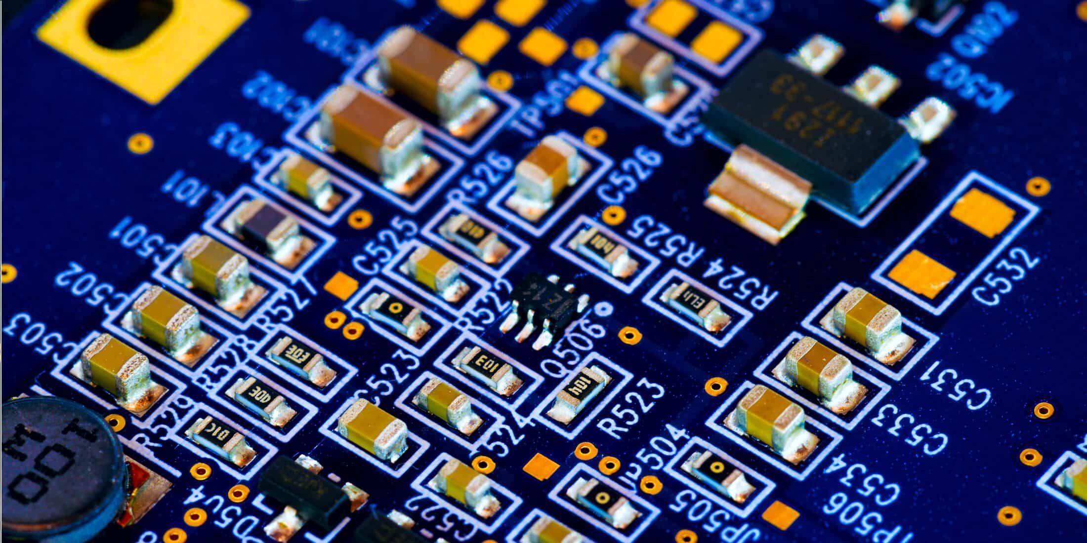
Keep up to date
Receive our monthly updates

