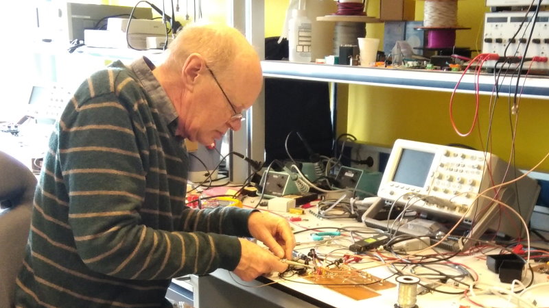
Jack Leijssen (Trainer)

Published on:
07 July 2021
Author:

Expert:

Jack Leijssen BSc
Trainer
A trip to Philips Semiconductors in the US made his reputation as an electronic design specialist within Philips. Ever since, Jack Leijssen has been spreading his holistic view on EMC, signal integrity and the like, both inside the company and out, through High Tech Institute in his training “Signal integrity of a PCB“.
Before his “Signal integrity of a PCB” training, Jack Leijssen’s career in electronic design really took off with the plane to the States he was put on at the turn of the millennium. “Philips Semiconductors was making cable modem chips there, based on a reference design from Philips CFT in America. But they couldn’t get the design to pass the EMC test. They had issues with the emission and the signal-to-noise ratio. Working as an electronic designer for CFT in Eindhoven, I was sent to help them out. It took me a year and a dozen round trips, but I solved the problems.”
'The IC designers screwed up and I got to clean up their mess'
“The IC designers screwed up and I got to clean up their mess,” recounts Leijssen. “They failed to adequately separate the analog and digital parts on the chip. Fixing that was not an option as that would have meant that they would have to start all over again. I had to look for solutions outside the chip. Moving the power supply, for example. And with all kinds of resistors, I was able to curb the currents, thereby reducing the crossover between the digital nets and improving the signal-to-noise ratio to the analog part. I fixed the IC design screwups on the board level.” With this, he cemented his reputation as an electronic design specialist within Philips.
Out of the box
Leijssen spent the formative years of his professional life at the famous Natuurkundig Laboratorium (Natlab). “I started there in 1975, maintaining and repairing spectrum analyzers. In 1986, I switched to the electronics design group, which at the time was largely populated by analog experts. The work, however, was getting increasingly digital. As no one wanted to do it, they offloaded it to me – being the new guy and one of the few who had gained some experience in microcontroller programming at school. Back then, I wasn’t a big fan of digital electronics either, so I volunteered for another project no one wanted to do – the ion implanter.”
A part of the infamous Megachip project, the ion implanter could be used to contaminate silicon with a wide range of periodic elements to create three-dimensional transistors. “Many people were put off by the radioactive and toxic materials we worked with and the megavolts we used to accelerate ions across 20-30 meters to write the small patterns in the wafer. Not me. I had the best time there. Being the only electronics engineer among mostly chemists, I could basically do anything I liked as no one was knowledgeable enough to correct me. I also learned a lot. I had some brilliant supervisors from my Natlab department, who taught me to think out of the box – which has been very instrumental to me in the rest of my career.”
The 2.5 years at the ion implanter were followed by a string of projects. Leijssen: “I was sent to Geldrop, where Philips was working on its Domestic Digital Bus, D2B, in a failed effort to set the standard for connecting consumer devices. After that, I moved to the Digital Compact Cassette, DCC – not a big success either, although it landed Philips a profitable front-row seat in MPEG. Since 1993, except for a few stints elsewhere, I’ve basically been deployed at ASML, developing analog electronics but also DSPs – for the wafer scanner prototype, among other things.”
Meanwhile, Leijssen went from the Natlab to CFT, to Research, to Innovation Services, which recently changed its name to Engineering Solutions. “I’ve never had to apply for a job,” he says, smilingly. “I just had to move my chair.”
Practical examples
The CFT-commissioned trip to Philips Semiconductors in the US, one of the “stints elsewhere,” set the stage for Leijssen’s side job as a trainer. “After I solved their problems, they proposed that I return on a regular basis to teach my American colleagues about stuff like EMC, signal-to-noise ratio, signal integrity and power integrity. I declined but it did trigger me to put together a presentation for Philips, which later developed into a training course. Within the company, I must have taught it a hundred times by now, to colleagues but also management. All new employees at Philips Engineering Solutions are required to take it.”
Through High Tech Institute, Leijssen also teaches the course outside Philips. “It targets true electronics engineers who run into design issues on a daily basis. The training is about making them aware that things like EMC emission, EMC immunity, signal-to-noise ratio, signal integrity, power integrity and noise classification mustn’t be viewed separately; they’re all linked together. I haven’t had many EMC specialists in my class because they tend to focus on only one aspect, and that’s not how it works. You can’t optimize for one and forget about the others.”
Taking this holistic view, Leijssen shows the participants what a printed circuit board needs to look like. “A data bus has a relatively low EMC footprint, but a clock line has a big EMC effect, exceeding all the limits. Such a clock line is therefore best placed on an inner layer, while it’s perfectly fine to put a data bus signal on an outer layer,” he illustrates. “One of the assignments in the training is to make a PCB with a very simple piece of electronics on it and encase it, first in plastic and then in metal. How does that affect the electrical characteristics? What happens when you put all the inputs on one side and all the outputs on the other side? Actually, that’s the worst thing you can do. I want the participants to get a feeling for all the electrical intricacies.”
Because of its practicality, Leijssen’s “Signal integrity of a PCB” training is actually more like a workshop. “I’m drawing a lot on personal experience. Being bound to NDAs for my recent assignments, I use examples from years ago, like the American job. But also the work we did for Bang & Olufsen. They set the bar extremely high, certainly for a consumer electronics company but even for medical standards: demanding a 100 dB signal-to-noise ratio and performing ESD tests at 16 kilovolts, where 2 kV is normal for consumer devices and 8 kV is common for medical equipment. The examples might not be new, but they’re definitely not outdated.”
Keep things simple
Although Leijssen has seen a change for the better over the years, there’s still some missionary work to do. “I’m part of a little club tackling the really tough EMC problems within Philips. We used to get a lot of calls for help from people running into electrical trouble nearing the end of a project. I’ve seen my share of project plans outlining a year of development followed by one week of EMC optimization, while you really should be doing this at the start. Yes, it makes it more expensive, but we’re talking about products that end up in homes or even hospitals. It’s gotten much better, although I still have a bone to pick once in a while.”
“Another positive trend,” Leijssen notes, “is that the board designs are getting simpler. There’s a growing awareness among chipmakers that they need to solve the problems themselves, instead of unleashing them on the PCB. So we’re seeing more and more signal integrity facilities being incorporated on chip, making the lives of electronics designers much easier. And then it’s up to them to also keep things simple on the board level. Why use eight layers when four is enough? Why use both sides of a PCB when you can put all the components on one side? Why choose a thin board that has a high risk of breaking when a thicker, more robust one does the trick equally well? It’s exactly this awareness that I aim to raise in my training.”
This article is written by Nieke Roos, editor in chief of Bits&Chips.
Recommendation by former participants
By the end of the training participants are asked to fill out an evaluation form. To the question: 'Would you recommend this training to others?' they responded with a 8.7 out of 10.
High Tech Institute organizes the 'Signal integrity of a PCB' training as a 2,5-day training.
Keep up to date
Receive our monthly updates

