Lectures supported by practical demonstrations and a final design case. Course notes.
Electronic systems are becoming faster, denser, and more power-hungry, making Power Distribution Network (PDN) design increasingly complex. With more supply voltages, tighter timing and noise margins, and rising interconnect density, power integrity can no longer be treated separately from signal integrity and EMC. A well-designed PDN is now essential for maintaining signal quality and electromagnetic compatibility. This course addresses board-level power distribution from a power integrity perspective, using minimal math and practical examples.
This course stands out due to:
- Product-design focus: The clear emphasis on the entire PDN path—from IC to PCB layout—directly supports product designers;
- IC <> PCB Interface insight: This bridging of roles between IC and board designers helps teams align across design domains, which is often overlooked but critical for real-world integration.
- Real-time problem solving with PI analysis to mitigate EMI/EMC by managing return paths and decoupling strategies
- Tool-neutral, practical approach: vendor-independent positioning makes the training accessible and adaptable to different company environments.
- Experienced instructor blending process and hands-on techniques: The mix of theory, tools, and direct application ensures content is retained and implemented effectively.
This training is available for open enrollment as well as for in-company sessions. For in-company sessions, the training can be adapted to your situation and special needs.
Objective
After the course, the participant will have basic knowledge of power integrity on board level and will be able to:
- determine the design requirements of a power distribution network;
- design a decoupling network impedance profile;
- select type, value and amount of decoupling capacitors to optimize performance and minimize cost;
- determine the effect of board layout and stack up on power distribution and how to optimize it;
- determine where to place decoupling capacitors;
- perform an analysis of a power distribution network;
- select tools to perform PDN simulations.
Target Audience
This course is intended for electronic designers, board and IC designers, system architects. Educational level: At least BSc in electronics or physics. Prior knowledge on EMC is not required. The focus of the course is on board design and on the interface between the board and its IC’s. IC designers need to know how to interface an IC to a board and on its effect on the power distribution on the board and within the IC.
Program
Introduction
- Functions of a Power Distribution Network (PDN)
- Power delivery issues: Voltage fluctuations, timing errors
- Sources of power supply noise: Core and IO circuits
- Power distribution noise: Time and frequency domain
Power Distribution Network (PDN) Components
- DC-DC converter: Types, properties and model for PI analysis
- Bypass Capacitors: Characteristics, parasitics and models of various capacitor types
- Planes and traces: Low frequency model, high frequency response, resonances
PDN design procedure
- Target impedance, transient currents, chip and package effects, design from chip to DC-DC converter
Layout considerations
- Mounted inductance of capacitors, effect of traces, vias, planes
- Stackup selection, power plane location and separation
PDN impedance design
- Various methods, high frequency effects of capacitor location and plane size, determine value and amount of decoupling capacitors needed
- Interaction of power integrity, signal integrity and EMC
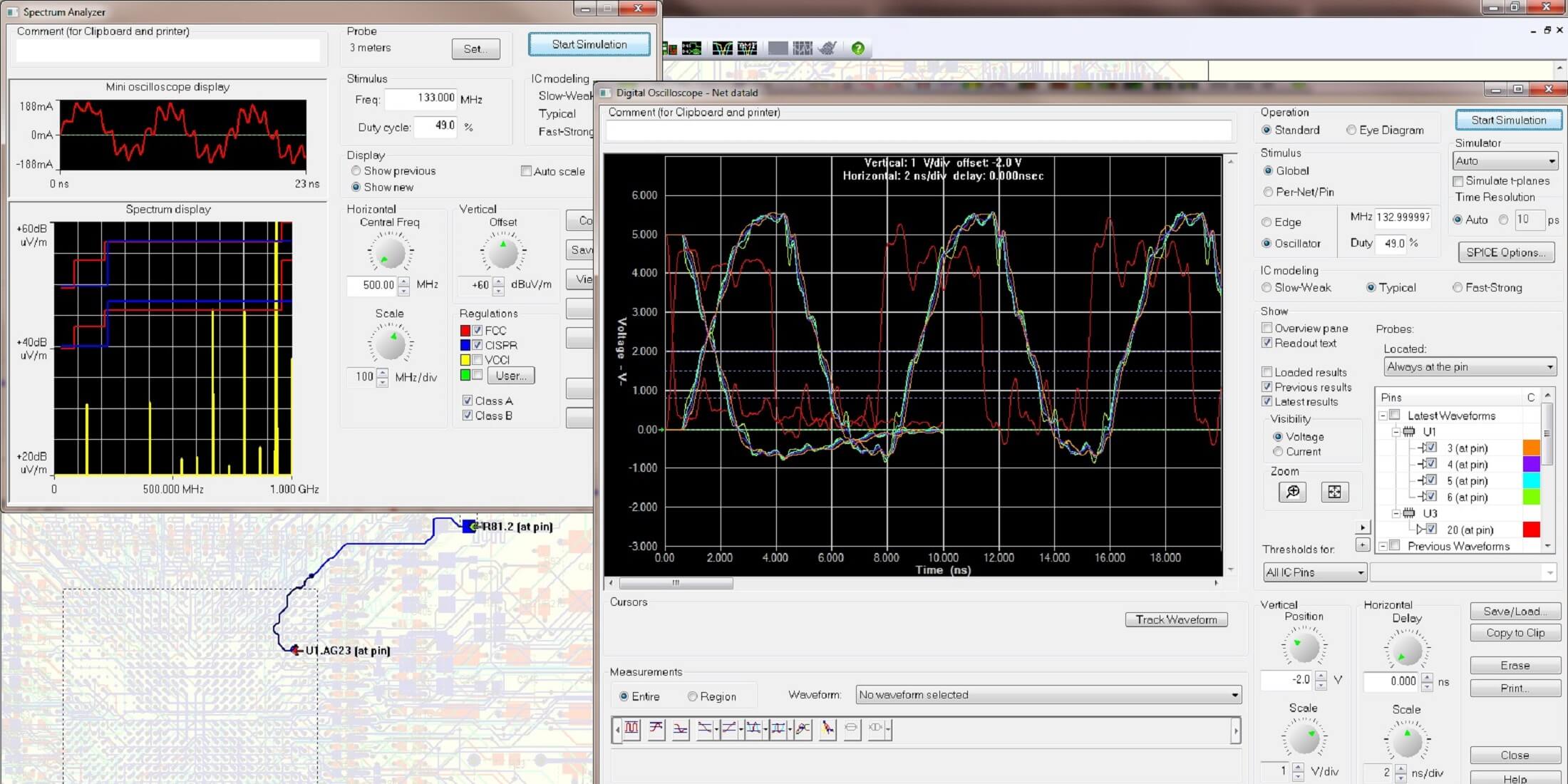
Simulation of a PDN
- Spreadsheets and SPICE simulation
- Advanced PI simulation: Pre- and post layout tool
PDN design example (exercise)
- Apply course knowledge in an exercise to design a PDN from beginning to end
Methods
Certification
Participants will receive a High Tech Institute course certificate for attending this training.
Course Reviews


