Erik Jan Marinissen PDEng. MSc. - trainer

Published on:
18 November 2020

When he was a student, he didn’t have the slightest interest in chips, let alone in testing them. Now, Erik Jan Marinissen is an authority in the IC test and design-for-test arena and even teaches on the subject.
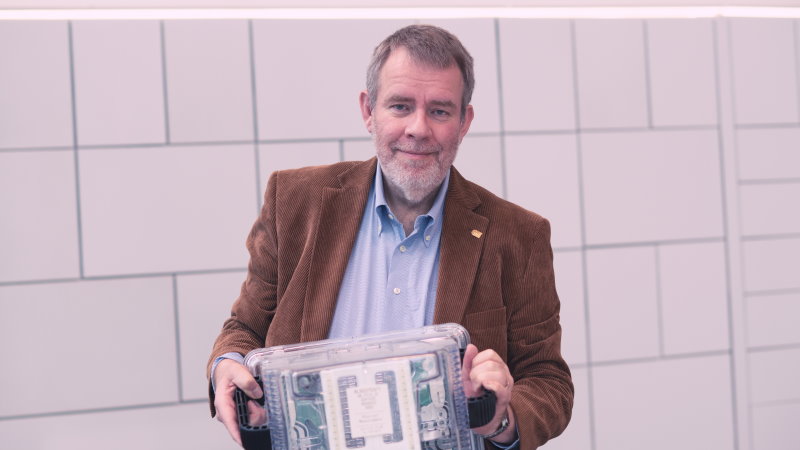
Last year, when Erik Jan Marinissen heard that his papers on Design for Test at the IEEE International Test Conference (ITC) had made him the most-cited ITC author over the last 25 years, he didn’t believe it. “I had skipped a plenary lunch session to set up a presentation that I would give later that day when passers-by started congratulating me. For what, I asked them. They explained that it had just been announced that I’m the most-cited ITC author over the past 25 years. Well, I thought, that can’t be right. Of course, I had presented a couple of successful papers over the years, but surely the demigods of the test discipline – the people I look up to – would be miles ahead of me,” tells Marinissen.
Back at home, Marinissen got to work. He wrote a piece of software that sifted through the conference data to produce a ‘hit parade’ of authors and papers. The outcome was clear: not only was he the most-cited author, but his lead over his idols was also actually quite substantial. ITC being the most prominent scientific forum in his field, there was no question about it: Marinissen is an authority in the test and design-for-test (DfT) disciplines (see inset “What’s design-for-test?”).

Credit: Imec
Once he was certain there had been no mistake, Marinissen felt “extremely proud. I’ve won some best-paper awards over the years, but they typically reflect the fashion of the moment. What’s popular one year, may not be anymore the next. My analysis confirms this, actually: not all awarded papers end up with a high citation score. Being the most-cited author shows that my work has survived the test of time; it’s like a lifetime achievement award.”
What’s design-for-test?
A modern chip consists of millions or even billions of components, and even a single one malfunctioning can ruin the entire chip. This is why every component needs to be tested before the chip can be sold. It’s turned on and off, and it needs to be verified that it changed state.
The hard part is: you can’t exactly multimeter every transistor as you’d do with, say, a PCB. In fact, the only way to ‘reach’ them is through the I/O, and a chip has far fewer I/O pins than internal components. Indeed, the main challenge of testing is to find a path to every component, using that limited number of pins.
This task is impossible without adding features to the chip that facilitate testing. Typically, 5-10 percent of a chip’s silicon area is there just to make testing possible: adding shift-register access to all functional flip-flops, decompression of test stimuli and compression of test responses, on-chip generation of test stimuli and corresponding expected test responses for embedded memories. Design-for-test (DfT), in its narrow definition, refers to the on-chip design features that are integrated into the IC design to facilitate test access.
Colloquially, however, the term DfT is also used to indicate all test development activities. This includes generating the test stimulus vectors that are applied in consecutive clock cycles on the chip’s input pins and the expected test response vectors against which the test equipment compares the actual test responses coming out of the chip’s output pins. Chip manufacturers run these programs on automatic test equipment in or near their fabs.
'I soon realized how wrong I was about testing. It’s actually a diverse and interesting field! '
Diverse and interesting
Verifying the calculations that entitled him to a prestigious award might be considered an instinct for someone who has dedicated his life to checking whether things work correctly, but Marinissen and testing weren’t exactly love at first sight. “As a computer science student at Eindhoven University of Technology, I didn’t have much affinity with chips or electrical engineering. We CS students used to look down on electrical engineers, actually. Electrical engineers are only useful for fixing bike lights, we used to joke. I’m sure they felt similarly about us, though,” Marinissen laughs.
Testing seemed even less appealing to Marinissen, for reasons he thinks are still true today. “If you don’t know much about the field, it may seem like testers are the ones cleaning up other people’s messes. That’s just not very sexy. For IC design or process technology development, it’s much easier to grasp the creative and innovative aspects involved. Even today, I very rarely encounter students who have the ambition to make a career in testing from the moment they set foot in the university.”
It took a particular turn of events for Marinissen to end up in testing. “I wanted to do my graduation work with professor Martin Rem because I liked him in general and because he worked part-time at the Philips Natuurkundig Laboratorium, which allowed him to arrange graduation projects there. Like most scientists in those days, I wanted to work at Philips’s famous research lab. But, to my disappointment, professor Rem only had a project in testing available. I reluctantly accepted, but only because I wanted to work with the professor at the Natlab.”
“I soon realized how wrong I was about testing. It’s actually a diverse and interesting field! You need to know about design aspects to be able to implement DfT hardware, about manufacturing to know what kind of defects you’ll be encountering and about algorithms to generate effective test patterns. It’s funny, really. Initially, I couldn’t be any less enthusiastic about testing, but by now, it has been tattooed on my forehead.”
Stacking dies
After finishing his internship at the Natlab in 1990, Marinissen briefly considered working at Shell Research but decided that it made more sense to work for a company whose core business is electronics. He applied at the Natlab, got hired but took a two-year post-academic design course first. Having completed this, Marinissen’s career started in earnest in 1992.
“At Philips, my most prominent work was in testing systems-on-chip containing embedded cores. A SoC combines multiple cores, such as Arm and DSP microprocessor cores, and this increases testing complexity. I helped develop the DfT for that, which is now incorporated in the IEEE 1500 standard for embedded core test. When the standard was approved in 2005, many people said it was too late. They thought that companies would already be set in their ways. That wasn’t the case. Slowly but surely, IEEE 1500 has become the industry default.”
Marinissen is confident the same will eventually happen with another standard he’s helped set up. He worked on this after transferring from Philips, whose semiconductor division by then had been divested as NXP, to Imec in Leuven in 2008. He actually took the initiative for the IEEE 1838 standard for test access architecture for three-dimensional stacked integrated circuits himself. He chaired the working group that developed the standard for years until he reached his maximum term and someone else took the helm. The standard was approved last year.
“Stacking dies was a hot topic when I was hired at Imec. Conceptually, 3D chips aren’t dissimilar from SoCs: multiple components are combined and need to work together. By 2010, I’d figured out what the standard should look like, I’d published a paper about it and I thought: let’s quickly put that standard together. These things always take much longer than you want,” Marinissen sighs.
His hard work paid off, though. Even before the standard got its final approval, the scientific director at Imec received the IEEE Standards Association Emerging Technology Award 2017 “for his passion and initiative supporting the creation of a 3D test standard.”
Credit: Imec
Flipping through the slides
As many researchers do, Marinissen also enjoys teaching. He accepted a position as a visiting researcher at TUE to mentor students who – unlike himself when he was their age – take an interest in DfT. At an early stage, he also got involved with the test and DfT course at Philips’ internal training center, the Centre for Technical Training (CTT). “Initially, most of the course was taught by Ben Bennetts, an external teacher, but I took over when he retired in 2006. I remember having taught one course while still at NXP, but not a single one for years after that – even though Imec allowed me to. There just wasn’t a demand for it.”
“Then, in 2015, all of a sudden, I was asked to teach it twice in one year. Since then, there has been a course about once a year.” By then, the training “Test and design-for-test for digital integrated circuits” had become part of the offerings of the independent High Tech Institute, although, unsurprisingly, many of the course participants work at companies that originate from Philips Semiconductors. “Many participants have a background in analog design or test and increasingly have to deal with digital components. I suppose that’s understandable, given the extensive mixed-signal expertise in the Brainport region.”
“I might be the teacher, but it’s great to be in a room with so much cumulative semiconductor experience. Interesting and intelligent questions pop up all the time – often ones I need to sleep on a bit before I have a good answer. It’s quite challenging, but I enjoy it a lot. As, I imagine, do the students. I’m sure they prefer challenging interactions over me flipping through my Powerpoint slides.”
From begrudgingly accepting a graduation assignment to sharing his authoritative DfT expertise in class – the young Erik Jan Marinissen would never have believed it.
Recommendation by former participants
By the end of the training participants are asked to fill out an evaluation form. To the question: 'Would you recommend this training to others?' they responded with a 8.6 out of 10.
Get to understand the role and importance of testing for manufacturing defects in the overall IC product creation process. Take a look at the 3-day “Test and design-for-test” training.
Keep up to date
Receive our monthly updates

